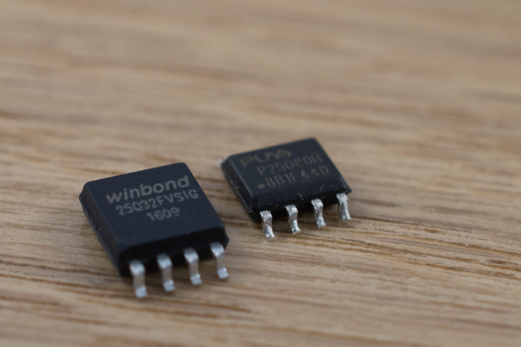
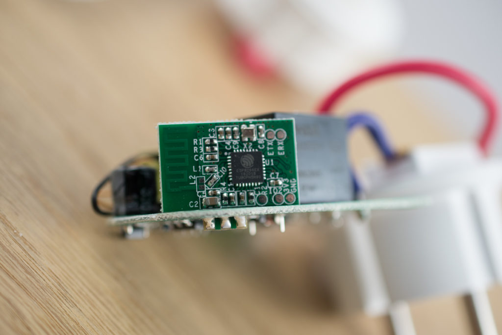
The Sonoff S26 WiFi-Plug/Switch uses a ESP8266 micro-controller and 1 MB of memory for its firmware. It is possible to replace the default EEPROM IC with a bigger one. This comes in handy, when using Tasmota and OTA-upgrades, since the upgrade needs to be locally stored, before it can be installed.
The 32 Mbit (4 MB) EEPROM used here, is a 25Q32FVSIG.
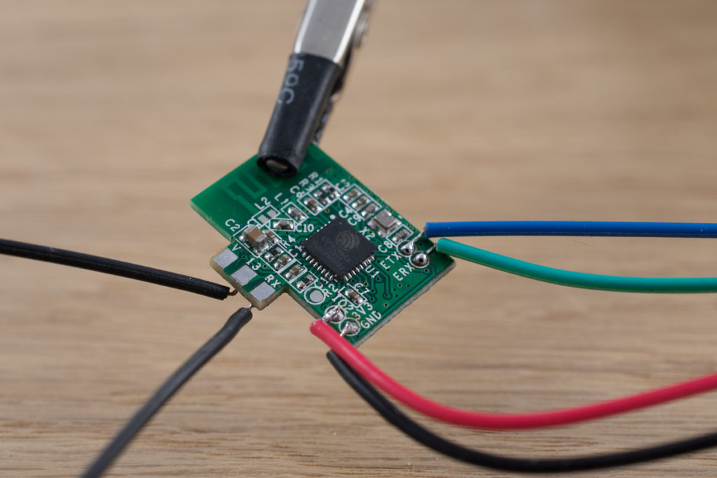
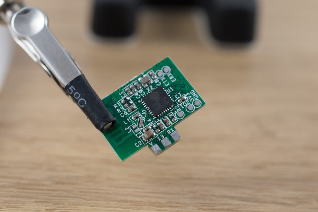
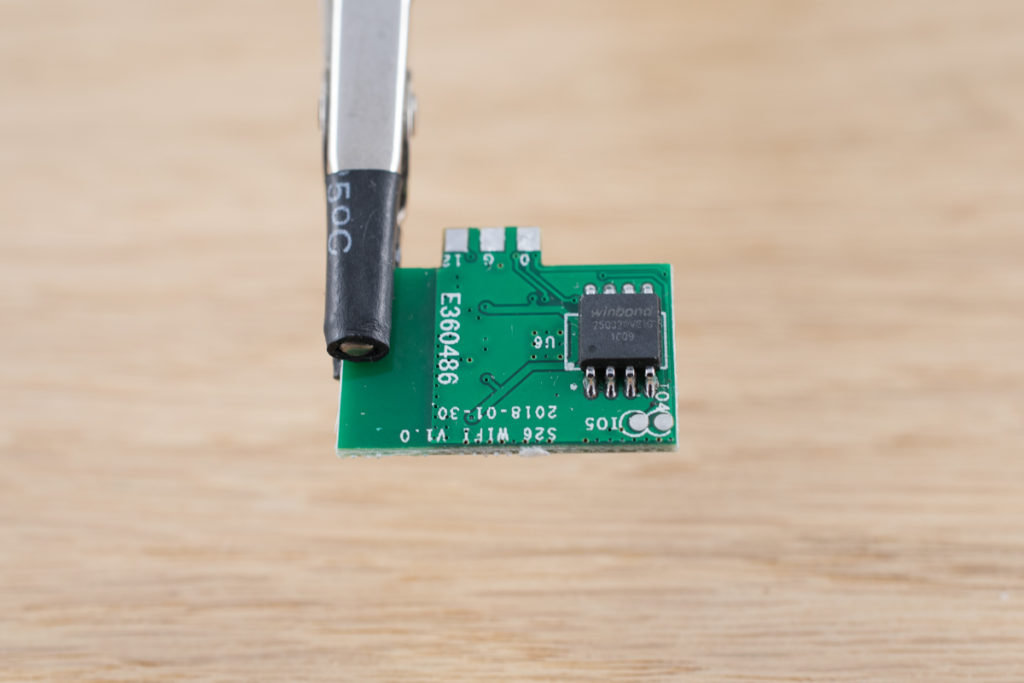
To get to the EEPROM, the small PCB needs to be removed from the main PCB. This can be done using a simple vacuum plunger and some solder wick with flux. All the solder pads on both PCBs should be cleaned afterwards.
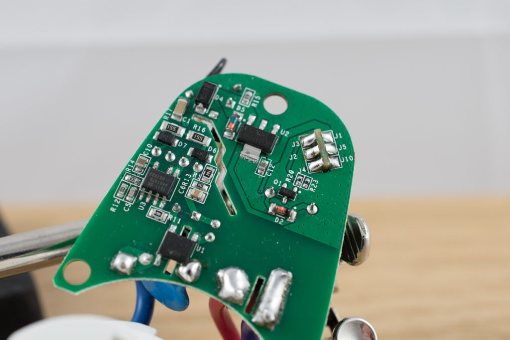
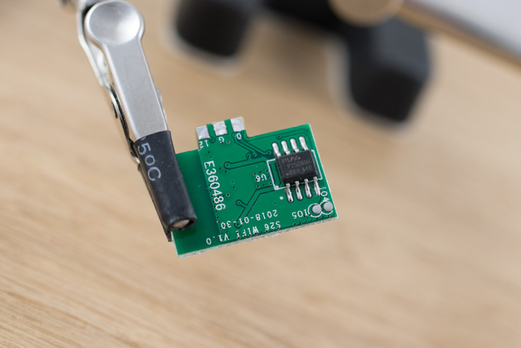
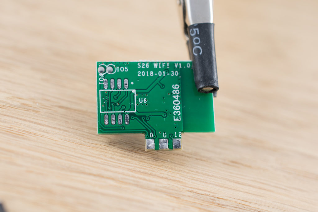
After removing the module, the backside containing the EEPROM is accessible. This IC needs to be removed first. I used a hot air gun, but it should also be possible to create a “solder blob” on both sides to remove all pins at the same time. After removing the component, the pads need to be cleaned up.
To put the new IC in, make sure, that pin 1 (the dot) matches the markings on the PCB. Then put some solder on one of the pads, hold the new EEPROM IC in place and reheat the solder. Now the IC should be fixated. After that, all the pins can be soldered easily with a small tip soldering iron. Another possibility would be a heat gun and some solder paste.
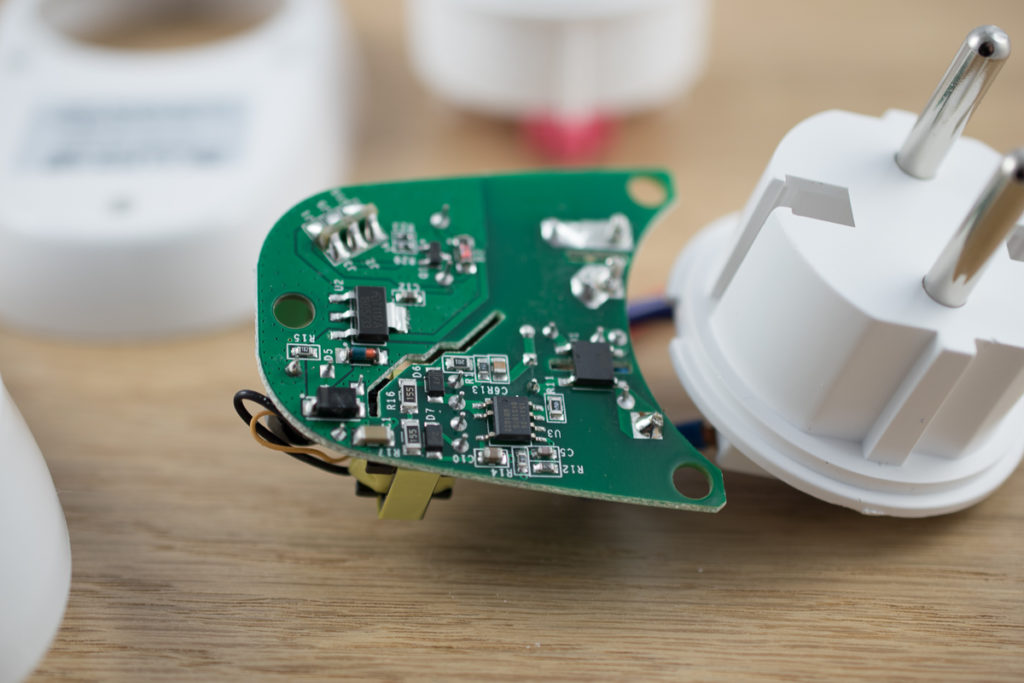
Before resoldering the small PCB to the big one, I recommend flashing and testing the new memory first. Because the button is on the main PCB, the “0” pad and the “G” pad on the board, need to be temporarily shorted with some wire, while powering the ESP8266 up, to put it in flash mode. Obviously the relay and LEDs can’t be used/tested in this state, but WiFi should work fine. Keep in mind, that most firmwares need to be configured accordingly before compiling, to access the whole memory range.